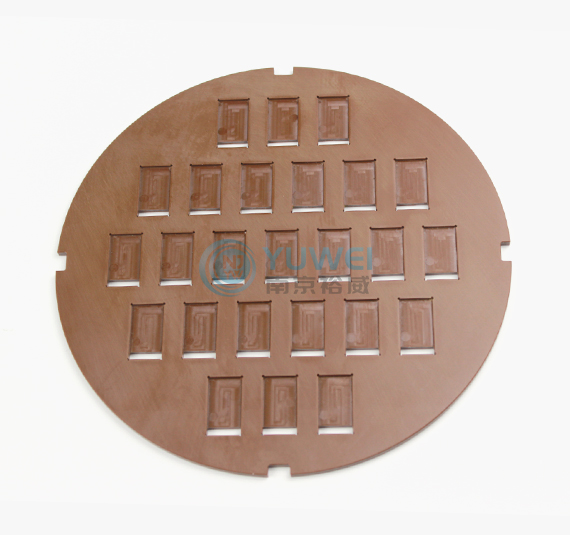
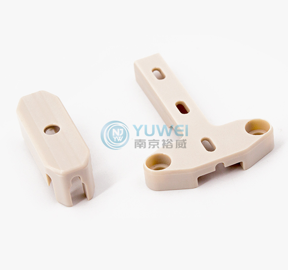
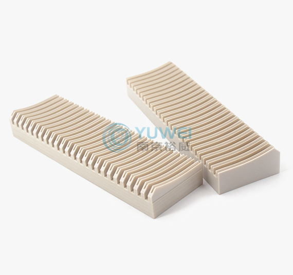
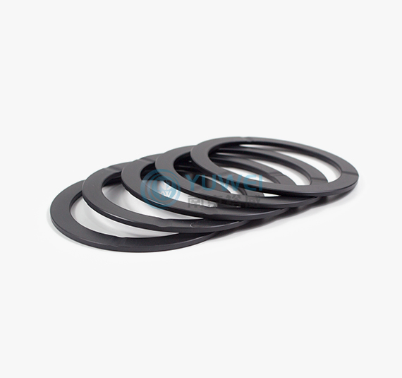
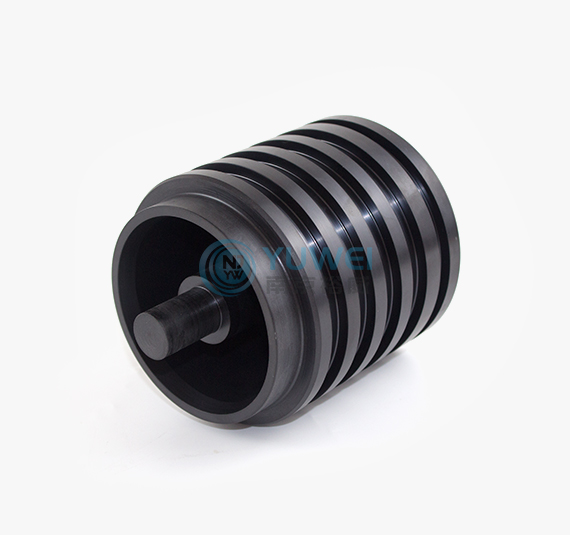
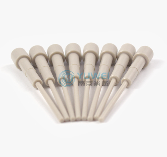
PEEK material is commonly used to manufacture wafer bearer, electronic insulating film and various connection devices, in addition to wafer bearer insulation film, connector, printed circuit board, high temperature connector, etc.


The semiconductor industry is moving towards larger wafers, smaller chips, narrower lines and line width sizes. PEEK polymer materials have obvious advantages in wafer manufacturing, front-end processing, processing and inspection, and back-end processing.
PEEK has the characteristics of high temperature resistance, wear resistance, corrosion resistance, low volatilization, low extraction, low moisture absorption, environmental protection and flame retardant, stable size, flexible processing, etc. It is widely used in computers, mobile phones, circuit boards, printers, light-emitting diodes, batteries, switches, connectors, hard disk drives and other electronic devices.